Could FPGA IP be headed to an SoC near you?
November 08, 2016
The more integrated, the better. That's truer in the embedded space now than ever before. For proof, look at the system on chip (SoC) landscape. SoC i...
The more integrated, the better. That’s truer in the embedded space now than ever before. For proof, look at the system on chip (SoC) landscape.
SoC integration has increased steadily over the past 20 years, originally including embedded memory and power management blocks and now incorporating everything from analog and mixed-signal IP to graphics and digital signal co-processors to security and connectivity subsystems (Figure 1). For higher performance applications the next step in this progression is to enable SoCs with hardware acceleration capabilities, ushering in the next generation of SoC IP – the embedded field-programmable gate array (eFPGA).
[Figure 1 | The evolution of system on chip (SoC) IP integration.]
Accelerating towards embedded FPGA IP
Introduced in the 1980s, the flexibility of FPGAs made them immediately applicable to designs that required transistor-transistor logic (TTL) integration and programmable I/O, as off-the-shelf application-specific standard products (ASSPs) and application-specific integrated circuits (ASICs) were not always equipped with the ports needed for a given system. Coupled with increasing connectivity demands over the ensuing years, that flexibility saw FPGAs used to connect processor arrays in the data center and also deployed as separate co-processors to compute complex, custom parallel workloads in a variety of signal processing applications. The broader use and exposure lead to FPGA density, performance, and cost improvements, and the market for the technology ballooned from $14 million n 1987 to nearly $5.4 billion in 2013.
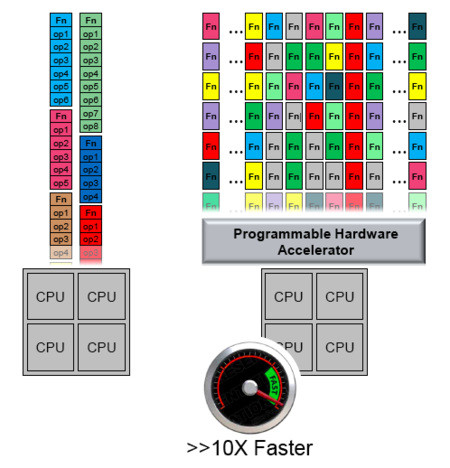
As today’s data center and networking applications continue to drive a relentless demand for lower latency and higher performance, chipmakers have started to investigate the benefits of integrating FPGA IP directly into their SoC designs. Once thought to be too difficult and too expensive, the compute advantages of implementing programmable hardware acceleration blocks into an SoC are undeniable, as rather than relying on the unscalable, sequential processing paradigms of multicore CPUs, FPGAs are capable of executing entire functions in a single clock cycle (Figure 2). Intel alone provides a twofold example of this trend, as 2015 saw the company buy FPGA giant Altera to maintain its dominance in the data center market, and earlier this year start shipping the Intel Xeon Processor E5 with an integrated Altera Arria 10 FPGA that is said to provide a 70 percent increase in performance-per-watt efficiency, a 20 percent improvement over workloads run on the x86 core, and the flexibility to be reprogrammed to meet the growing demand for specialty chips from Intel customers.
[Figure 2 | Integrating a programmable hardware acceleration block via FPGA IP into an SoC can provide as much as a 10x processing boost over the traditional serial processing of additional CPUs.]
But why should all the fun be limited to Intel? It isn’t. Recently, Achronix Semiconductor released its Speedcore eFPGA IP.
Harnessing the power of flexibility
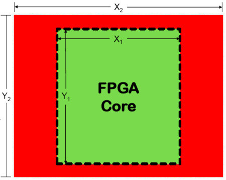
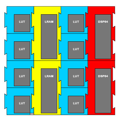
Speedcore eFPGA IP has been three years in the making, much of which dealt with the challenge of making an inherently flexible technology, well, rigid enough to be rapidly implemented in of a wide range of SoC designs. To achieve this, Achronix engineers adopted a modular architecture approach that allowed for the efficient development of uniquely sized FPGA core structures, with all functional blocks adopting standard interface routing and unit sizing (Figure 3). As a result, Speedcore IP can be envisioned as a “Lego-like” composition of IP that supports multiple timing closure methodologies, the option for shared or separate power supplies without power sequencing requirements, and the ability to build variable width data paths. These parameters are configurable through Achronix’ ACE design tool suite that further enables chip designers to specify die size, quantity of lookup tables (LUTs), digital signal processing (DSP) blocks, memory blocks, and I/O port connections (Figure 4).
[Figure 3 | Achronix Speedcore embedded FPGA IP (eFPGA) is based on a “Lego-like” architecture that allows SoC designers to customize the number of look-up tables, DSP and memory blocks, I/O ports, and power supplies.]
[Figure 4 | Speedcore eFPGA IP is configurable using Achronix’ ACE design tools, which support common electronic design automation (EDA) flows.]
While FPGA fabric can deliver significant horsepower to an SoC as described previously, embedding it as IP has several ancillary benefits that may not be immediately apparent. These are all derived from the fact that technologies such as Speedcore are implemented as IP rather than a discrete chip, resulting in board size, power, cost, and latency reductions.
First, in terms of board size, approximately 50 percent of a typical FPGA’s footprint is dedicated to programmable I/O, SerDes connectors, and interface controllers, all of which are dispensable as the necessary I/O is present as part of the core FPGA fabric that uses direct wire connections to an SoC (Figure 5). Additionally, peripheral components such as power regulators, clock generators, and separate cooling devices can be eliminated.

[Figure 5 | By eliminating SerDes connectors, interface controllers, and other components required by a standalone FPGA, Speedcore eFPGA IP can provide reductions in board size, latency, power consumption, and cost.]
It follows that reduced printed circuit board (PCB) footprint, the lack of a separate chip, and the removal of other supporting components serve to lower overall system costs (according to Achronix, as much as 90 percent). Further, fewer devices coupled with performance increases that allow processing tasks to complete more quickly also help minimize power consumption (by up to 50 percent, the company says).
But transitioning back to performance, the removal of SerDes connectors that add latency also permits wide register interface paths to be constructed directly from the FPGA core and main CPU, minimizing communications bottlenecks associated with standalone FPGAs (Figure 6).

[Figure 6 | The lack of SerDes connectors in SoC designs leveraging eFPGA IP can yield significant latency reductions over discrete FPGA solutions.]
Could FPGA IP be headed into an SoC near you?
Speedcore eFPGA IP currently targets applications that require large amounts of parallel processing, such as digital front ends (DFEs) for 5G base stations, software-defined networking (SDN), and high-performance cloud computing, but as volumes ramp, can we expect to see this type of technology in more deeply embedded applications?
Robert Blake, President and CEO of Achronix Semiconductor believes so, stating that “there’s no reason why FPGA integration shouldn’t exist, and you may see smaller companies announce these technologies in lower performance [applications] with lower levels of integration.”
“Intelligence will migrate outward,” he continued. “If you can build high-end embedded FPGAs, you can build ones that are lower in performance and power optimized. The tool chains will be optimized over time and the gains of parallelism will be realized.”
Speedcore eFPGA IP can be licensed today, and is available on 16FF+ processes from TSMC now with 7 nm tapeouts slated for the first half of 2017.
For more information, visit www.achronix.com/Speedcore.


