Asking the right questions when selecting flash memory devices for industrial applications
February 01, 2017

Selecting flash memory devices, or solid-state drives (SSDs), for industrial applications is complex. Price-performance comparisons are of little use...
Selecting flash memory devices, or solid-state drives (SSDs), for industrial applications is complex. Price-performance comparisons are of little use because the demand-driven definition of performance hinges on a host of factors.
When it comes to standard IT applications, price-per-GB is a perfectly good purchase criterion for flash memory. In some cases, write and read speed is also considered. But if you have a need for flash memory devices for industrial applications, or you require memory cards for outdoor telecom applications, then your priorities are going to be different. If, as is often the case, capacity is not really an issue, robustness and durability certainly are. Endurance (i.e. flash media lifetimes) and retention (i.e. durability of saved data) are complex issues. Storage medium firmware and architecture both come into play here, as does the nature of the application. How will data be written? Or is the emphasis more on reading? If you have special requirements for flash memory, then you need to know exactly which questions to ask.
Background: Signs of aging
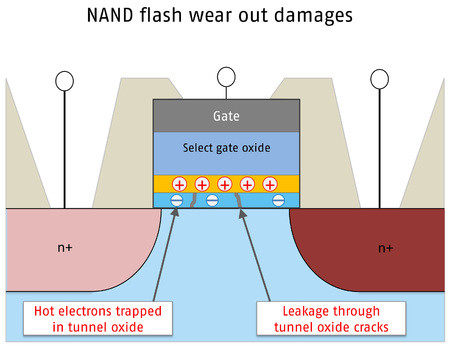
Typically, the cells of NAND flash devices only allow for a limited number of deletions. This is attributable to the fact that each time the tunnel effect is generated, the oxide layer, which normally prevents electrons from flowing off from the floating gate, accumulates high-energy electrons due to the extinguishing voltage. As a result, the threshold voltage changes over time to the point where ultimately the cell is no longer readable (Figure 1).

[Figure 1 | An aging cell: Electrons accumulate in the tunnel oxide layer, causing the threshold voltage to gradually change. Cracks in the tunnel oxide layer induce leakage current paths, permitting the charge to flow off. Read errors increase to the point where the block becomes a “bad block” that needs to be retired. ]
Another effect of aging is the formation of conductive paths in the oxide layer, causing the cell to gradually lose charge – and with it the hold bit. This effect, which is accelerated by exposure to high temperature, tends to occur particularly in cases where the number of allowed program/erase (P/E) cycles decreases, causing retention to decline dramatically. Hence, while both new single-level and multi-level cell (SLC and MLC) NANDs reliably provide 10 years of retention, this figure declines to only one year by the end of their lifetimes. But with MLC NANDs, this point is reached after 3,000 P/E cycles compared to after 100,000 with SLCs. This explains why SLCs are the preferred solution for sophisticated applications – and why low-cost triple level cell (TLC) NAND chips cannot be used for long-term storage. To write three bits per cell using this technology, you need eight distinct charge states, which is why degeneration becomes noticeable much sooner. In TLCs, the original one-year retention level declines to three months after only 500 P/E cycles.
Mitigating measures
The effects of physical damage to the chip are mitigated using various mechanisms. Given the fact that when a cell fails the entire block needs to be marked as “bad,” wear leveling ensures that all physical storage addresses undergo the same level of usage. But read errors point to more than just wear and tear. Each time data is written, the cells surrounding the programmed cell undergo stress (i.e. they become more energetic) – a phenomenon known as ‘program disturb.’ Over time, the cell voltage threshold increases, leading to read errors – which are fixed once the relevant block is erased. Reading also results in a form of stress known as ‘read disturb,’ whereby the adjacent pages accumulate the charge. Owing to the relatively low voltage involved, this effect is far less pronounced than with writing – nevertheless reading is prone to bit errors that must be corrected by error-correcting code (ECC) and fixed by deleting the relevant block. Interestingly, this effect is particularly pronounced in applications that read the same data repeatedly. This means that even within a read-only memory, blocks need to be deleted and pages repeatedly written for errors to be corrected.
How SSD endurance is measured
Manufacturers measure the lifetime of a flash memory device using two metrics: terabytes written (TBW) and drive writes per day (DWPD). TBW indicates the total amount of data that can be written during an SSD’s lifetime, whereas DWPD indicates the amount of data that can be written every single day during the warranty period. The problem with these benchmarks is that they are extremely complex, and users have no choice but to rely on the manufacturer’s specifications. Plus, it is unclear how relevant these specifications actually are when it comes to selecting the right data medium for a given application since the figure obtained is largely determined by a test workload. For example, tests of a Swissbit 480 GBP SSD resulted in a 1360, 912, or 140 TBW lifetime, depending on the measurement method used. The most striking result is achieved by measuring sequential writing. The second value (912) is yielded by a client workload, whilst the third (140) is derived from an enterprise workload. Both load tests constitute JEDEC standards. The client workload is based on the behavior of a computer user, and mostly generates sequential accesses. The enterprise workload, on the other hand, simulates the performance of a server in a multi-user environment that generates up to 80 percent random accesses.
Although theoretically these standards should allow for comparability, the problem is that many manufacturers simply do not indicate the underlying workloads and base their product information on sequential write values. And because, as the example shows, the latter can differ for enterprise workloads by a factor of ten, extreme caution is needed when it comes to remarkable and unclearly specified high endurance values.
Write amplification factor (WAF) reduction
The logical to physical mapping system, ECC, and a process called garbage collection to clear out blocks are all relevant mechanisms when it comes to understanding and ranking flash memory functionality and performance. A key term in this domain is write amplification factor, or WAF, which is the ratio between the user data derived from the host and the actual amount of data that is written to the flash memory device. Reducing WAF – a metric for flash controller efficiency – is key when it comes to ramping up SSD endurance. The workload factors that influence WAF comprise the difference between sequential and sequential and random accesses, or data block size relative to pages and block sizes. Two basic conditions must be satisfied: pages need to be written one after the other, and blocks need to be deleted as whole units. In the standard procedure, the mapping between logical and physical address relates to blocks. This is highly efficient for sequential data because the pages of a given block can be written sequentially. An example of this mechanism is continuously accumulated video data. However, pages are written in numerous different blocks for random data whereby every internal overwrite of a page requires an entire block to be deleted. This results in higher WAF and a reduced lifetime. Thus, page-based mapping is preferable for non-sequential data. In other words, the firmware ensures that data derived from disparate sources can be written sequentially to the pages of a single block. This reduces the number of deletions and thus prolongs lifetime and enhances write performance. The drawback of this method is that it results in a larger assignment table of the flash transition layer (FTL), though this can be compensated for by an integrated DRAM.

[Figure 2 | Comparison test: Compared to conventional products, the F-60 durabit is far more durable and has lower WAF. This is achieved via FTL in the DRAM and greater over-provisioning.]
Another factor that ramps up WAF is memory usage. The more data that is stored on a flash device, the more bits the firmware needs to move from one place to another. Page-based mapping is advantageous here as well. Manufacturers have yet another adjustment mechanism known as over-provisioning (i.e. the space of a flash memory device that is reserved solely for background activities) at their disposal. Seven percent of an SSD (the difference between binary and decimal values for gigabyte figures) is normally reserved for this purpose. But reserving 12 percent rather than 7 percent for over-provisioning is amazingly effective. For example, an endurance comparison (i.e. the TBW for enterprise workload) of two identical SSDs derived from MLC NAND chips has shown that the 60 GB Swissbit F-60 durabit achieved a 6.6x higher value than the same company’s 64-bit F-50 device. And in fact, the value is 10 times higher for the 240 GB and 265 GB versions.

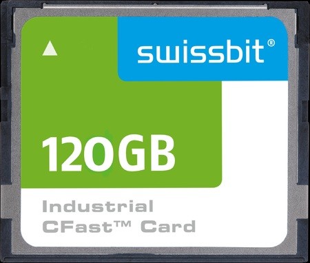
[Figure 3 | Shown here is the CFast F-60 durabit SSD.]
Conclusion and nine key questions to ask
SLC flash memory devices are in many ways the most robust solution for industrial applications, as well as for power outage protection. However, in many cases high-end MLC flash media is just as suitable for such purposes. Mechanical properties ranging up to military standards aside, when looking for an SSD solution, particular attention should be paid to the amount of effort the manufacturer puts into reducing WAF and extending product lifetime via firmware. Other factors that come into play are “data care management” measures for better retention and not to forget long-term availability of the modules that have been meticulously qualified for a given application.
Application requirements determine which factors you need to pay particular attention to in selecting an SSD. On request, Swissbit provides its customers with a Lifetime Monitor, a tool that calculates the endurance of a given SSD by analyzing its reads and writes. And as noted, even if price isn’t the determining factor, it’s useful to know whether you really need an eight times more expensive SSD, or whether MLC will suffice for your purposes.
Key questions to ask when selecting flash memory devices for industrial applications:
- Do I have specific physical requirements for vibration, resistance, and temperature range? – Industrial flash memory devices should, through the application of an appropriate qualification process, be able to show proof of high-quality material properties and good production and processing.
- Is the memory storage exposed to high temperatures for extended periods of time? – Because high temperatures weaken the readability of the cells faster, a product with data care functions should be chosen, which regularly refreshes the data.
- Is the intention to write and store a large volume of data on the data carriers over a long period of time? – If so, an SLC product should be chosen.
- Does the application predominantly require read access? – If yes, a product with data care functions should be chosen, which regularly refreshes the data.
- Does the application predominantly require write functionality? – Then a product with block-based mapping is suitable for sequential write functionality. For random requests, a product with page-based mapping should be selected.
- Is the capacity of the memory fully utilized? – For intensive use applications, the controller demands space for internal operations and over-provisioning can extend endurance.
- What workload has the provider specified for TBW or DWPD? – The comparison of data carriers is only possible through the indication of the workload benchmarks.
- Is a higher level of protection against data loss required? – For particularly critical applications, data care management and power fail protection are essential.
- Will the medium still be available in several years’ time? – The manufacturer should guarantee long availability so that the memory storage can be replaced without the need to requalify.
Swissbit AG


