Dev Kit Weekly: ADLINK’s NVIDIA® Jetson Nano™ based AI Camera Dev Kit
March 03, 2023
Sponsored Video
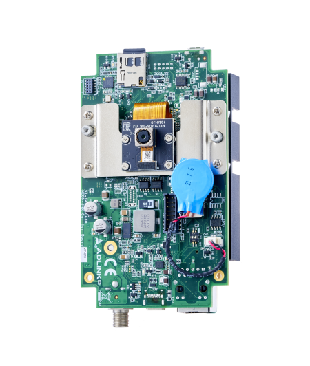
When you think of AI at the edge, what immediately comes to mind? If your answer has anything to do with monitoring safety-critical environments, like edge computer vision systems that oversee plants that house hazardous materials or factories full of autonomous robots, you’ve come to the right place. And this place is an introduction to ADLINK’s AI Vision Developer Kit built around the NVIDIA Jetson Nano module.

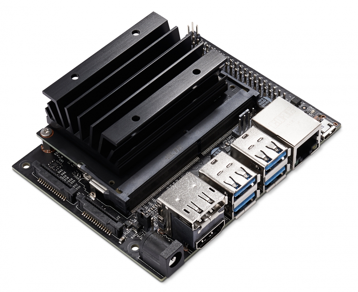
The AI Vision Developer Kit integrates a Sony 8 MP CMOS image sensor that captures 15 frames per second at 3280 x 2464 resolution, a heat spreader to cool the stack down, and pre-loaded software optimized for multiple edge AI applications to help you get Jetson Nano-based vision PoCs running in the blink of an artificial eye. The Jetson Nano levies a quad-core, 1.43 GHz Arm Cortex-A57 MPCore CPU and 921 MHz Maxwell GPU with 128 CUDA cores against vision workloads running on the kit, delivering up to 472 GFLOPs of performance in the kit’s 130 mm x 72 mm x 43.8 mm form factor.

Supporting these memory intensive workloads is 4 GB of 64-bit LPDDR4 memory and 16 GB of onboard eMMC storage, as well as, of course, multimedia interfaces for piping data in and out of the system. Much of this is handled by the truly remarkable onboard USB Type-C interface, which functions as a 30 fps 1920 x 1080 DisplayPort interface and power supply (should you choose not to use the 12-24 DC-in terminal), in addition to handling standard data transfers over integrated USB3 and USB2 lanes. There’s also 10/100/1000 Mb Ethernet brought out over an RJ45 LAN port, 8 DIOs and a UART off these headers, an additional USB OTG port, and a microSD slot for added data and development flexibility.
I mentioned that this kit comes with software. Specifically, it includes ADLINK’s Edge Vision Analytics (EVA) SDK, which is a low-code GUI-based development platform that includes plenty of tools and libraries that will have even the most inexperienced developers prototyping. There are two different open-source AI vision applications loaded on the Camera Dev Kit out-of-the-box: Pose Detection and Object Classification. These can be modified easily to support industrial worker safety and hazardous material monitoring applications, and code for those and other similar use cases is available to download for free from the EVA page on ADLINK’s website.


Of course, since it’s that easy to get started on application development, ADLINK wouldn’t leave you hanging on something like driver integration. To that end, V4L2 drivers and APIs and the Gstreamer multimedia processing framework are already built into the stack so you can maximize the Sony image sensor right away.
So if you need a vision PoC in a flash, with an AI Camera Dev Kit, a power source, a development PC, and half an hour you could have something to show your boss. To get one of your own you can request a quote from ADLINK on their website, or you could try your hand at winning this one right by entering this week’s raffle. The winner will get the whole kit delivered to their door for absolutely free.
To request a quote from ADLINK, visit the product page.


