High-Power Monolithic IC for System on a Chip
July 22, 2026
Blog
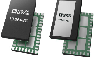
Power supplies for the integrated power management IC (PMIC) used in system on a chip (SoC) applications are required to meet a wide range of stringent performance requirements, including not only high output current capability, but also fast and small load transient response, low electromagnetic compatibility (EMC) characteristics, low temperature rise, and low input current during suspend modes.
Recent automotive systems widely employ electric control units (ECUs) to electronically control and manage mechanical subsystems using compact embedded computers. Each ECU is designed to execute a specific function, and modern vehicles incorporate numerous ECUs to support a broad range of control requirements. As functional consolidation progresses, multiple ECU functions are increasingly integrated, resulting in higher processing demands on the system on a chip (SoC) devices that perform centralized control. Consequently, the required supply current has risen sharply.
As shown in Figure 1, the SoC supplies various voltages generated by the integrated power management IC (PMIC) to internal blocks such as the CPU and MEMORY. The PMIC itself typically operates from a 3.3V supply. In automotive systems, the primary power source is generally a lead‑acid battery, which provides a nominal voltage of approximately 12V to 14V. The 3.3V rail for the PMIC is generated by the primary power IC, which is required to deliver load currents exceeding 10A. Because the PMIC has a relatively narrow allowable input‑voltage range, the output voltage of the primary power IC must maintain high accuracy, including tight control of ripple and load‑induced variations.
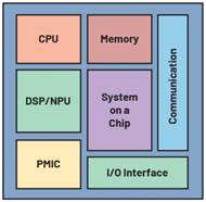
Figure 1. Diagram of an SoC.
Key Requirements for SoC Power
When a load current of more than 10A is required, a controller IC that drives external FETs is commonly used. To handle the large currents and the resulting heat dissipation, a controller IC—where the switching FETs are placed separately from the power IC—is advantageous. In general, a monolithic IC with integrated FETs is not suitable for such high‑current and high‑thermal‑stress applications. However, the LT8648S is a monolithic IC that can support the high‑current requirements of SoC applications, and it is already used on automotive ECUs as the power supply for PMICs in SoC.
Figure 2 shows PCB layout representations of evaluation boards for a controller IC and a monolithic IC. Compared with a controller IC that requires external FETs, a monolithic IC with integrated FETs clearly enables a significant reduction in PCB area.
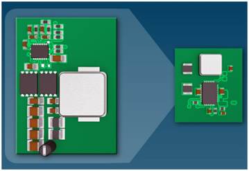
Figure 2. PCB layout of a controller IC and a monolithic IC.
As SoC performance continues to advance, the required supply current increases accordingly. While the LT8648S has been successfully mass produced and adopted in automotive systems as a PMIC power source, further increases in load current have created a need for enhanced thermal capability. The LT8648SP was developed to address this requirement. Conventional IC packages, as shown in Figure 3a, encapsulate the silicon die in resin, and heat is primarily dissipated through the bottom terminals into the PCB. In contrast, the LT8648SP exposes the silicon die on the top surface of the package (Figure 3b). Direct attachment of a heat sink to the exposed die enables highly efficient heat dissipation. As shown in Figure 4, the LT8648SP exhibits thermal performance comparable to the LT8648S when no heat sink is used; however, when a heat sink is attached, its temperature rise is less than half that of the LT8648S. This improvement allows the LT8648SP to support substantially higher load currents.
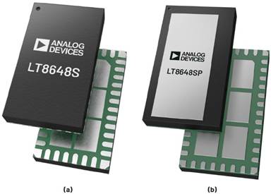
Figure 3. (a) LT8648S surface and (b) LT8648SP surface.
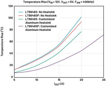
Figure 4. Temperature rise of the LT8648S and LT8648SP.
As noted earlier, SoCs demand extremely high load currents. As these currents increase, electromagnetic compatibility (EMC) challenges also intensify, necessitating additional filtering and external components, which increase system complexity. Primary power ICs, which are directly connected to the battery, have particularly significant EMC impact within the ECU and must exhibit excellent radiated emission (RE) and conducted emission (CE) characteristics. The LT8648S/LT8648SP incorporate Analog Devices’ patented Silent Switcher® 2 architecture. Silent Switcher technology reduces magnetic emissions by symmetrically placing input capacitors, as shown in Figure 5, thereby confining magnetic fields near the IC and significantly improving EMC performance. Silent Switcher 2 technology further enhances EMC by placing the input capacitors inside the package, right next to the silicon die (Figure 6). As a result, the LT8648S/LT8648SP comfortably satisfy the automotive EMC standard CISPR 25 Class 5, as demonstrated in Figure 7.
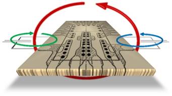
Figure 5. Silent Switcher structure.
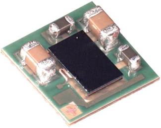
Figure 6. Inside the Silent Switcher 2 LT8609S.
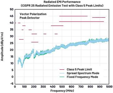
Figure 7. Radiated EMC performance of the LT8648S.
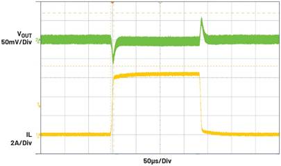
Figure 8. Load transient between a light load and a heavy load.
During vehicle operation, SoC processing loads fluctuate rapidly and significantly. Because the SoC’s input‑current demand varies accordingly, the power IC must exhibit robust load‑transient response. As shown in Figure 8, the LT8648S/LT8648SP rapidly return to the programmed output voltage with minimal overshoot and undershoot, even under large load‑current transitions. This characteristic is essential for PMICs supplying SoC, which allow only a narrow input‑voltage range.
When the vehicle is not operating, low quiescent current becomes critical. During suspend mode, the SoC periodically wakes to perform detection tasks and then returns to sleep—a behavior known as periodic wake‑up. In this mode, the LT8648S/LT8648SP must supply power with minimal consumption. ADI’s patented Burst Mode® operation enables significant reduction in light‑load current. Figure 9 illustrates the switching waveforms and inductor currents for Burst Mode and forced continuous mode. Burst Mode switches only when the output voltage falls below a defined threshold, rather than at a fixed frequency, thereby reducing switching events and maintaining high efficiency under light loads. During suspend mode, the SYNC pin should be set low to enable Burst Mode, while during normal operation it should be set high to enable forced continuous mode. Mode transitions can be performed seamlessly during operation without disturbing the output voltage.
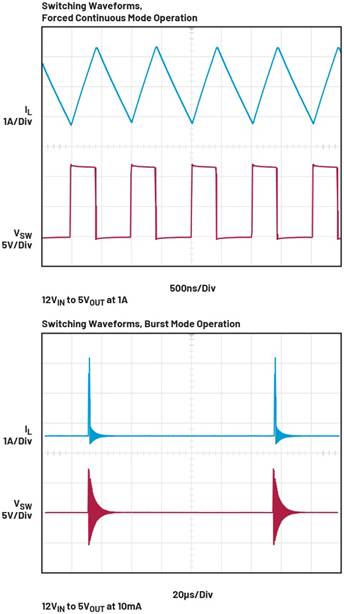
Figure 9. Switching waveform of forced continuous mode and Burst Mode.
As SoC performance continues to evolve, further increases in load current are anticipated. As shown in Figure 10, two LT8648S/ LT8648SP devices can be paralleled by connecting their inputs and outputs, thereby increasing the available load current. Even at load levels exceeding 30A, output‑voltage deviation remains minimal, as shown in Figure 11. The devices automatically interleave their switching phases, preventing EMC degradation during parallel operation.
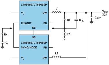
Figure 10. Paralleling two LT8648Ss.
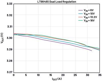
Figure 11. LT8648S load regulation in dual operation.
Conclusion
Although the LT8648S/LT8648SP are monolithic power ICs with integrated FETs, they support high output currents and deliver highly accurate, stable voltage across wide input‑voltage and temperature ranges. They also provide low EMC emissions and low quiescent current—both essential for automotive applications. The devices are therefore well suited for ECUs requiring compact size and high‑current capability.

Kazutaka Saito is a staff field applications engineer at Analog Devices. He has extensive experience supporting automotive customers, primarily in the field of power management ICs, gained through his work at Linear Technology (now part of Analog Devices) and Analog Devices. With many years of experience in the semiconductor industry, he has also been responsible for product development at a previous company.